ZHAW researchers develop chip for ultra-high resolution microscope
ZHAW researchers have developed a chip for a new measurement method using atomic force microscopy (AFM) as part of an Innosuisse project. This new method makes it possible to scan the surface far more quickly and gently, and it is suitable for organic samples and cell cultures of only a few nanometres in size. The manufacturer Nanosurf, which is based in Liestal in the canton of Basel-Landschaft, will now commercialise microscopes that use this measurement method.

With the newly developed WaveMode measuring mode for the DriveAFM atomic force microscope, Nanosurf has presented an innovation that facilitates swift and gentle analyses of a large number of different materials, including organic substrates such as cell cultures, DNA molecules and even viruses. The original technology behind atomic force microscopy (AFM), an ultra-high resolution type of scanning probe microscopy, was invented in Switzerland by the IBM scientists Gerd Binnig and Heinrich Rohrer in 1985. The two received the Nobel Prize in Physics for their research in 1986.
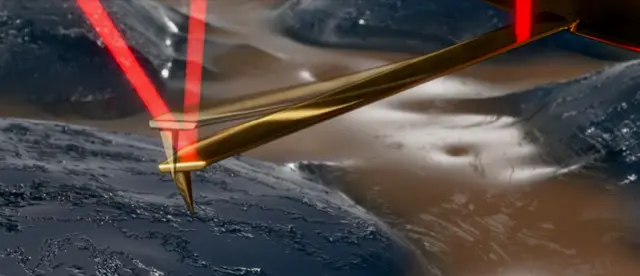
With existing AFM measurement methods, the cantilever (the lever arm, similar to a needle tip) “scratches” over the surface of the material being analysed, often damaging it and thus resulting in a lower resolution. For the new method developed at the Swiss Federal Institute of Technology Lausanne (EPFL), the cantilever is set in motion through photothermal excitation. The material is analysed merely by tapping it, resulting in a much faster and gentler process (photothermal off-resonance tapping). With an increased frame rate and improved results, structures in the nanometre range can be made visible.