Nanoscale Characterization
Correlating device parameters to nanoscale properties is one of our research goals and a great challenge in the field. We operate a nano-imaging lab with combined Raman, photoluminescence, and AFM capabilities. For electron microscopy, we are using the ETH electron microscopy center to perform FIB SEM.
Correlative Microscopy

With our LabRAM system from Horiba, we perform confocal photoluminescence mapping with a resolution given by the diffraction limit. Measuring a spectrum at each position, we obtain information on inhomogeneities on the micrometer scale. These can be related for instance to composition of the investigated materials and defect concentrations. Using our Linkam stage, the measurements can also be performed as a function of temperature.
An atomic force microscope is connected to the optical system, allowing for colocalized optical spectroscopy and atomic force microscopy to correlate luminescence and topography information. Electrical AFM modes such as conductive AFM and KPFM provide information on conductivity and surface potential, respectively. Dependent on the mode, resolutions in the 10s of nm to nm range can be reached. Measuring in the dark vs. under light, photoconductivity and surface photovoltage can be determined.
Measurements can be conducted on surfaces of films or on device cross sections.
An environmental chamber is available to perform experiments in N2 atmosphere.
Major Measurement Techniques
- Confocal PL in the visible range with lasers (405 nm, 532 nm, and 633 nm) as excitation sources
- Confocal Raman spectroscopy
- Atomic force microscopy (AFM)
- Kelvin probe force microscopy (KPFM)
- Conductive AFM
3D Focused Ion Beam Scanning Electron Microscopy
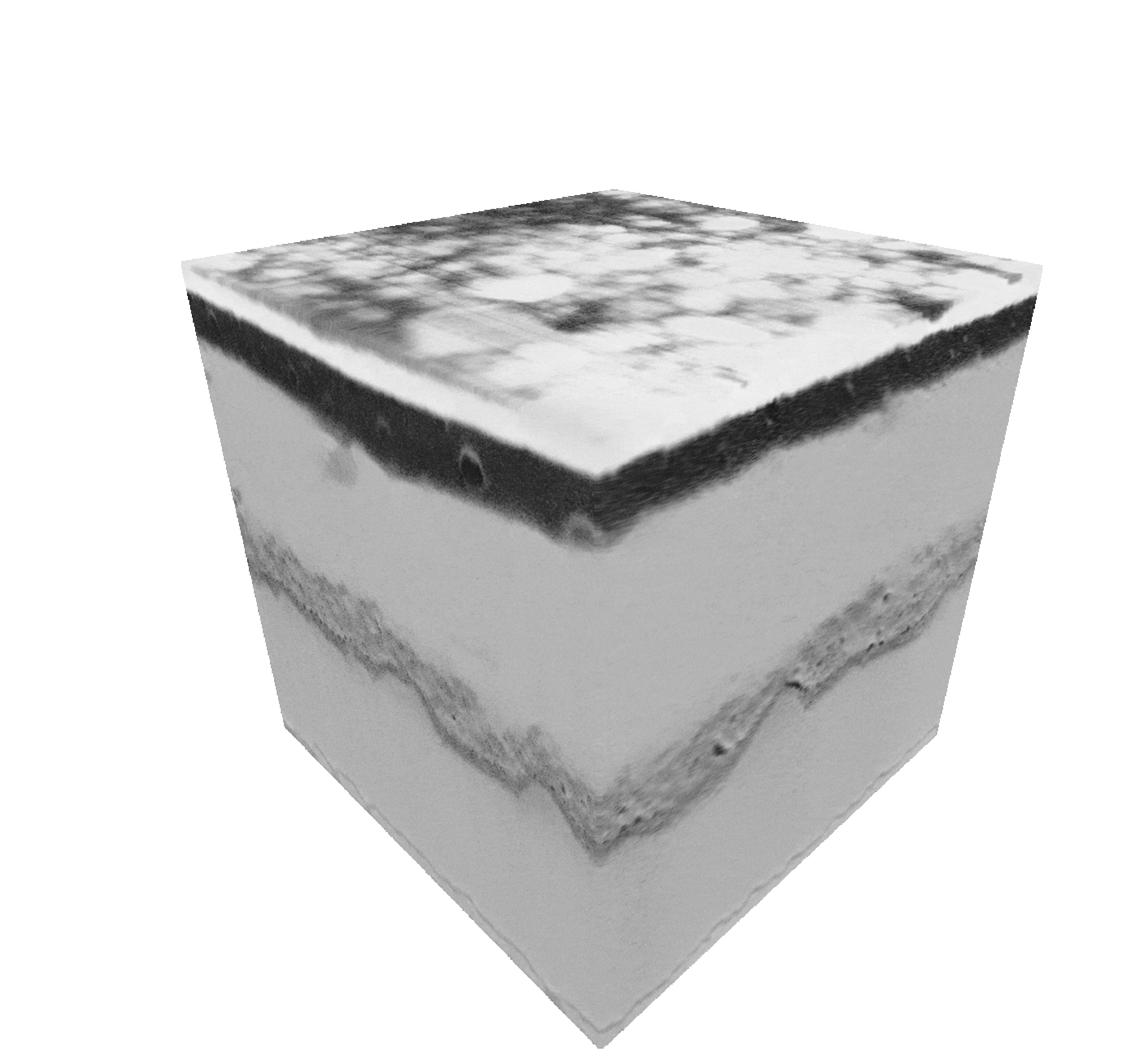
Our research group is at the forefront of advancing the understanding of perovskite solar cells by employing 3D Focused Ion Beam Scanning Electron Microscopy (FIB-SEM). We specialise in creating detailed volumetric models that reveal the interactions between layers and defect formations within solar cell devices during manufacturing. This allows us to optimise the device layer morphology and reverse engineer degradation pathways at the nanoscale after stress-testing which may be buried between interfaces.
The experiments are performed at ScopeM.